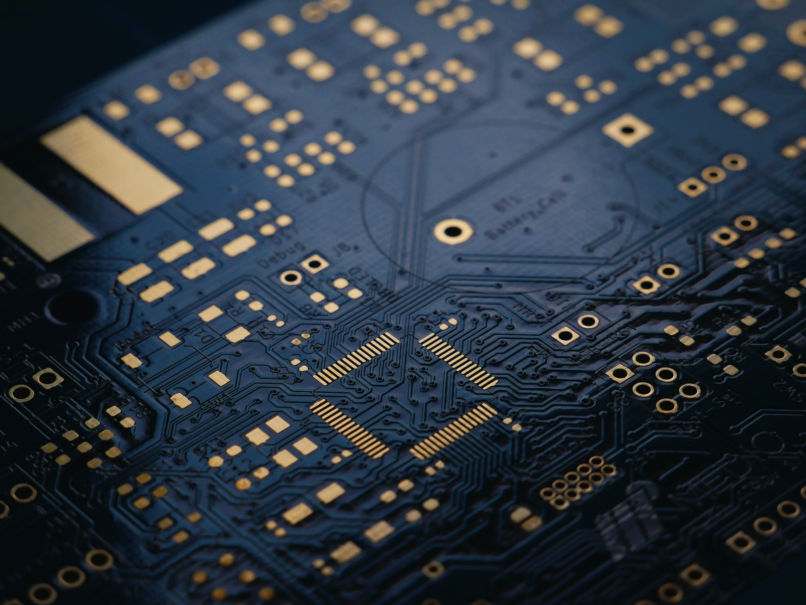
PCB prototyping is a necessary part of the electronic product development cycle.
Our online PCB prototype shop can turn even the most complicated designs into working prototypes quickly and with minimal fuss.
What is PCB prototyping?
When you are making a new electronic product or component, you need to know that the finished article will perform as you expect it to.
Computer modelling can help, but you don’t really get a true representation of performance before you hold a working model in your hands.
Making a prototype PCB is your first chance to see a functional version of your design in the flesh.
Before going to volume or batch production, this is your chance to iron out any design kinks, improve the allocation of materials and impress stakeholders or investors with an interest in your project.
The team at Hi5 Electronics have decades of experience turning ideas and PCB designs into fully functional prototypes. We’d love to do the same for yours.
Why is PCB Prototyping important?
PCB prototyping is the most cost-effective way of testing your design.
It can be very costly to correct a major design flaw once your design has already gone into volume production. Not to mention how time-consuming this correction would be.
PCB prototyping also give you an opportunity to optimise your design so that it is as efficient as possible, correcting any errors that might affect the quality or efficiency of your final product.
With more complex products that have several functions and PCBs, design engineers often like to test single boards or functions individually. Using a prototype allows them to test basic functions by themselves before adding in more layers of complexity. This not only helps improve the performance of specific functions, but it can also help isolate and diagnose issues later in the design process.
A working prototype also helps unlock additional business advantages.
Although you can create a minimum viable product using basic technology like a breadboard, using a PCB creates a more permanent design that looks professional.
If you can show buyers and investors a professional-looking working model, rather than a series of schematics, you have a better chance of landing that purchase order or investment.
There are times when PCB prototyping can feel unnecessary. This is particularly true when staring down the barrel of very tight deadlines.
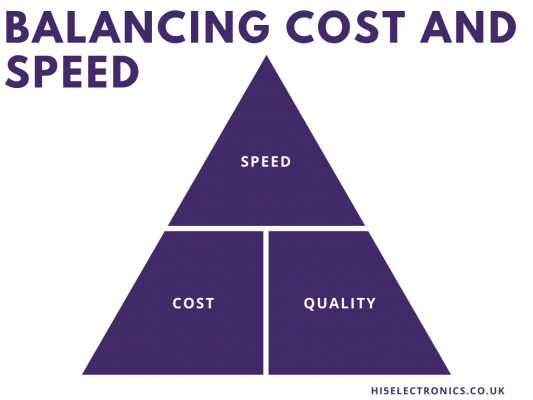
For this reason, speed and turnaround time are often very important in the PCB prototyping process.
PCB prototyping turnaround time
Designers are often under pressure to meet deadlines and get projects finished as quickly as possible. And because a PCB may have to go through several rounds of prototyping, the speed of prototyping is essential.
As always though, increased speed means a trade-off in either cost or quality. To get a prototype PCB turned around in a few days, you will either pay a premium or the quality of the finished product will suffer. Because most designers can’t afford to compromise on quality, the prices will usually rise.
During volume production, engineers are usually willing to compromise on timescales in order to get high-quality boards made at the best possible price. This type of manufacturing normally takes place in Asia or Eastern Europe, where labour is cheaper, but delivery takes longer.
To benefit from faster turnaround time, PCB prototyping normally takes place in the UK. UK operators like Hi5 Electronics are able to offer the fastest turnaround times and high-quality products at a reasonable price.
We also offer different costs for different turnaround times. Use the calculator in our online shop to find out how much your prototype PCB will take to produce.
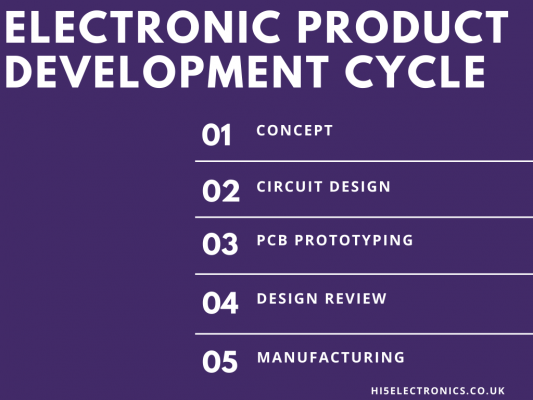
PCB Prototyping Process
In this section, we will detail some of the most important parts of the PCB prototyping process.
The easiest way is to work with a specialist PCB prototype partner. Companies like Hi5 Electronics will work closely with you, guiding you through each step of the way.
With decades of industry experience and high levels of customer service, Hi5 Electronics is ideally suited to guide you through each stage of the PCB prototyping process. For help and advice with anything in this guide, please speak to a member of the team today. Call: 01706 647 006
Start with a schematic
A schematic is a basic blueprint of your circuit, laying out all of the components and how they link together.
You can create a schematic using basic circuit software. Some software will automatically convert these schematics into PCB files, making life easier for designers.
Optimise the design
When you are designing a PCB, there are lots of things you can do to optimise the design. It is best to identify different parts of a circuit and keep those grouped together.
For example, on a circuit that has a power supply, an audio input and an audio output, it is best to keep each function grouped together to keep the traces between components short. Otherwise, these long traces could cause interference and noise.
You should also seek to make sure that the path of electrical current is as linear as possible and that each section of the circuit is supplied with power by traces of equal length to ensure each section gets an equal share of voltage.
At this stage, you will also need to think about how the PCB will interact with the final product. If you will have an LED near to a power switch, for example, you will need to think about how this will look on the final design.
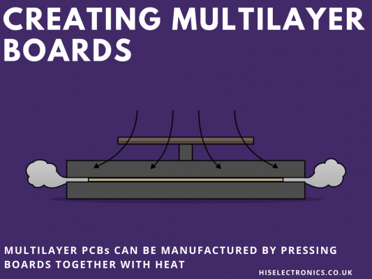
Multilayer PCBs
Large circuits can be difficult to fit on a single-layered PCB because it is hard to route the traces without them intersecting. In these cases, you can use double or multi-layered PCBs with copper-plated holes connecting the top and bottom layers.
Submitting your PCB design
To submit your design for prototyping and obtain a quote for PCB prototypes, you will need to prepare some information about the design. The information includes:
- The number of layers you need
- Board thickness
- Copper thickness and weight
- Minimum tracing and spacing
- Minimum hole size
- Surface finish
- Soldermask and colour
- Silkscreen legend and colour
- Drill file NC Excellon
- Drill file tool list
Design files can be submitted using a range of different software packages. We will convert the files into Gerber RS-274X, which is the optimum file type.
If we are converting your file to RS-247X, be sure to include positive Gerber layers, an NC Excellon drill file, a drill tool list and information on the aperture, solder mask and silkscreen.
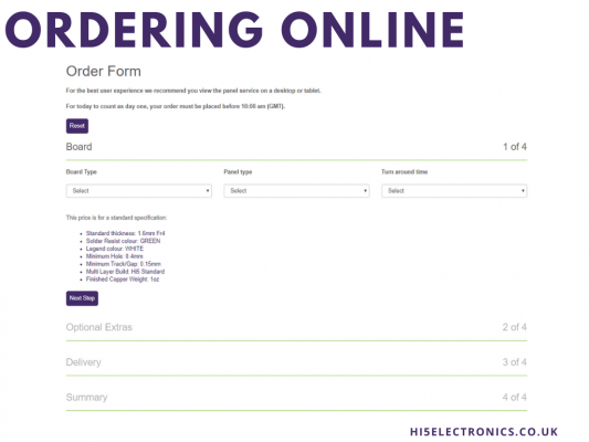
On the Hi5 Electronics shops, you can also set a range of customisable features, including:
- Board type
- Panel size
- Turnaround time
- Standard/premium finishes
- Hole size
- Testing requirements
- Solder resist
- Delivery time (extended delivery discount)
Want a quote? Visit our online shop and fill in your details for a no-obligation quote. Want more information? Speak to a member of the team today. Call: 01706 647 006.